
- 146
- 8 546 351
Phil’s Lab
Germany
Приєднався 10 лют 2007
Analog and digital electronics design, PCB design, control systems, digital signal processing, and more!
Website - www.phils-lab.net
Patreon - www.patreon.com/phils94
Hardware Design Courses - phils-lab-shop.fedevel.education
Website - www.phils-lab.net
Patreon - www.patreon.com/phils94
Hardware Design Courses - phils-lab-shop.fedevel.education
PCB Chip Antenna Hardware Design - Phil's Lab #139
Basics of integrating a PCB chip antenna into hardware designs. Tips on what to watch out for, antenna selection, matching, and PCB design. PCBs by PCBWay www.pcbway.com
[SUPPORT]
Hardware design courses: phils-lab-shop.fedevel.education
Course content: www.phils-lab.net/courses
Patreon: www.patreon.com/phils94
[GIT]
www.github.com/pms67
[SOCIAL]
philslabyt
[LINKS]
Chip vs Trace Antennas: e2e.ti.com/cfs-filesystemfile/__key/CommunityServer-Discussions-Components-Files/307/6683.PCBvsTrace_5F00_ant.pdf
Six Hidden Costs in a Wireless SoC Design: www.silabs.com/documents/public/white-papers/six-hidden-costs-in-a-wireless-soc-design.pdf
Chip Antenna Selection: www.johansontechnology.com/chip-antenna-selection
5 Things to Consider When Choosing an Antenna: www.mobilemark.com/5-things-to-consider-when-choosing-an-antenna/
Antenna Selection Guide: www.ti.com/lit/pdf/swra161
Impedance Matching: www.analog.com/en/resources/technical-articles/radio-frequency-impedance-matching-calculations-and-simulations.html
Understanding Matching Networks: www.allaboutcircuits.com/textbook/radio-frequency-analysis-design/selected-topics/understanding-matching-networks/
w2aew YT Channel: @w2aew
Stitching Vias: resources.altium.com/p/everything-you-need-know-about-stitching-vias
[TIMESTAMPS]
00:00 Introduction
01:14 PCBWay
01:47 Trace vs Chip Antenna
04:40 Pre-Certified Modules
05:58 Chip Antenna Selection
12:33 Matching, Tuning, Schematic
20:26 Footprint
22:31 PCB
31:53 Outro
Переглядів: 10 592
Відео


STM32H7 ADC + DMA + Timer Firmware Tutorial - Phil's Lab #138
Переглядів 15 тис.21 день тому
ADC set-up with DMA streams and sampling timer for STM32 microcontrollers. Tips on working with H7's D-cache and memory protection unit (MPU). PCBs by PCBWay www.pcbway.com [SUPPORT] Hardware design courses: phils-lab-shop.fedevel.education Course content: www.phils-lab.net/courses Patreon: www.patreon.com/phils94 Free trial of Altium Designer: www.altium.com/yt/philslab Altium 365: www.altium....

2-Layer PCB Design Tips - Phil's Lab #137
Переглядів 34 тис.Місяць тому
Tips for designing with only two copper layers on a PCB (layer assignment, component placement, routing, GND jumps, RF considerations). PCBs by PCBWay www.pcbway.com [SUPPORT] Hardware design courses: phils-lab-shop.fedevel.education Course content: www.phils-lab.net/courses Patreon: www.patreon.com/phils94 Free trial of Altium Designer: www.altium.com/yt/philslab Altium 365: www.altium.com/alt...
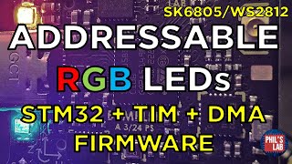
STM32 + RGB LEDs Firmware Tutorial (TIM + DMA) - Phil's Lab #136
Переглядів 14 тис.Місяць тому
How to control addressable RGB LEDs (SK6805, WS2812) using PWM timers with DMA in C using STM32 MCUs. PCBs by PCBWay www.pcbway.com [SUPPORT] Hardware design courses: phils-lab-shop.fedevel.education Course content: www.phils-lab.net/courses Patreon: www.patreon.com/phils94 Free trial of Altium Designer: www.altium.com/yt/philslab Altium 365: www.altium.com/altium-365 [GIT] www.github.com/pms67...

FPGA/SoC SD Card + PetaLinux (Zynq Part 6) - Phil's Lab #135
Переглядів 11 тис.2 місяці тому
AMD/Xilinx Zynq-7000 SoC SD card hardware configuration, SD card partitioning/formatting, and boot set-up for PetaLinux. PCBs by PCBWay www.pcbway.com [SUPPORT] Hardware design courses: phils-lab-shop.fedevel.education Course content: www.phils-lab.net/courses Patreon: www.patreon.com/phils94 Free trial of Altium Designer: www.altium.com/yt/philslab Altium 365: www.altium.com/altium-365 [GIT] w...
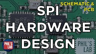
SPI Hardware & PCB Design - Phil's Lab #134
Переглядів 24 тис.2 місяці тому
SPI implementation tips (pull-ups, termination, schematic and PCB design). PCBs by PCBWay www.pcbway.com [SUPPORT] Hardware design courses: phils-lab-shop.fedevel.education Course content: www.phils-lab.net/courses Patreon: www.patreon.com/phils94 Free trial of Altium Designer: www.altium.com/yt/philslab [GIT] www.github.com/pms67 [SOCIAL] philslabyt [LINKS] PCB Arts Meet-Up: www....

PCB Silkscreen & Solder Mask 101 - Phil's Lab #133
Переглядів 12 тис.3 місяці тому
Basics, tips and tricks for working with silkscreen and solder mask in PCB designs. PCBs by PCBWay www.pcbway.com [SUPPORT] Hardware design courses: phils-lab-shop.fedevel.education Course content: www.phils-lab.net/courses Patreon: www.patreon.com/phils94 Free trial of Altium Designer: www.altium.com/yt/philslab Free search engine for the best quality components from Octopart: octopart.com/ Le...
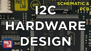
I2C Hardware & PCB Design - Phil's Lab #132
Переглядів 37 тис.3 місяці тому
I2C implementation tips (pull-up resistor sizing, bus capacitance, schematic gotchas, and PCB design). PCBs by PCBWay www.pcbway.com [SUPPORT] Hardware design courses: phils-lab-shop.fedevel.education Course content: www.phils-lab.net/courses Patreon: www.patreon.com/phils94 Free trial of Altium Designer: www.altium.com/yt/philslab [GIT] www.github.com/pms67 [SOCIAL] philslabyt [L...

PCB Design Final Touches (Tips & Checklist) - Phil's Lab #131
Переглядів 19 тис.4 місяці тому
Tips when finishing up a PCB design before manufacturing (polygon pours, solder mask, silkscreen, teardrops, etc.). PCBs by PCBWay www.pcbway.com [SUPPORT] Hardware design courses: phils-lab-shop.fedevel.education Course content: www.phils-lab.net/courses Patreon: www.patreon.com/phils94 Free trial of Altium Designer: www.altium.com/yt/philslab Free search engine for the best quality components...
QA403 Audio Analyzer Tutorial (Noise, SNR, THD+N, ...) - Phil's Lab #130
Переглядів 11 тис.4 місяці тому
How to measure noise floor, signal-to-noise ratio, total harmonic distortion, frequency response, and more of an audio electronic system using the QA403 audio analyzer. PCBs by PCBWay www.pcbway.com [SUPPORT] Hardware design courses: phils-lab-shop.fedevel.education Course content: www.phils-lab.net/courses Patreon: www.patreon.com/phils94 [GIT] www.github.com/pms67 [SOCIAL] Instagram: instagra...
STM32 Bluetooth Firmware Tutorial (Bring-Up) - Phil's Lab #129
Переглядів 28 тис.5 місяців тому
Firmware and bring-up tutorial for custom hardware based on STM32WB BLE microcontrollers. PCBs by PCBWay www.pcbway.com [SUPPORT] Hardware design courses: phils-lab-shop.fedevel.education Course content: www.phils-lab.net/courses Patreon: www.patreon.com/phils94 Free trial of Altium Designer: www.altium.com/yt/philslab Free search engine for the best quality components from Octopart: octopart.c...
KiCad 7 STM32 Bluetooth Hardware Design (2/2 PCB) - Phil's Lab #128
Переглядів 144 тис.5 місяців тому
Step-by-step schematic and PCB design tutorial for STM32WB-based hardware (USB, RF, power) in KiCad 7. (Part 2 of 2) (Part 1: ua-cam.com/video/nkHFoxe0mrU/v-deo.html) PCBs by PCBWay www.pcbway.com [SUPPORT] Hardware design courses: phils-lab-shop.fedevel.education Course content: www.phils-lab.net/courses Patreon: www.patreon.com/phils94 Tag-Connect: www.tag-connect.com/solutions-target-devices...
KiCad 7 STM32 Bluetooth Hardware Design (1/2 Schematic) - Phil's Lab #127
Переглядів 121 тис.6 місяців тому
Step-by-step schematic and PCB design tutorial for STM32WB-based hardware (USB, RF, power) in KiCad 7. (Part 1 of 2 / Part 2: ua-cam.com/video/PlXd3lLZ4vc/v-deo.html) PCBs by PCBWay www.pcbway.com [SUPPORT] Hardware design courses: phils-lab-shop.fedevel.education Course content: www.phils-lab.net/courses Patreon: www.patreon.com/phils94 Tag-Connect: www.tag-connect.com/solutions-target-devices...
Real-Time Impulse Response Simulation in Software (STM32 DSP) - Phil's Lab #126
Переглядів 14 тис.6 місяців тому
Impulse response system modelling, simulation, and real-time implementation on an STM32 microcontroller for a guitar cabinet. PCBs by PCBWay www.pcbway.com [SUPPORT] Hardware design courses: phils-lab-shop.fedevel.education Course content: www.phils-lab.net/courses Fedevel courses: www.fedevel.com Free trial of Altium Designer: www.altium.com/yt/philslab Patreon: www.patreon.com/phils94 [GIT] w...
Class D Audio Amplifier Hardware Design - Phil's Lab #125
Переглядів 25 тис.7 місяців тому
Class D audio amplifier basics, part selection, schematic and PCB design, and test. PCBs by PCBWay www.pcbway.com [SUPPORT] Hardware design courses: phils-lab-shop.fedevel.education Course content: www.phils-lab.net/courses Fedevel courses: www.fedevel.com Free trial of Altium Designer: www.altium.com/yt/philslab Patreon: www.patreon.com/phils94 [GIT] github.com/pms67 [SOCIAL] Instagram: instag...
Comb Filters & Delay Lines in Software (STM32) - Phil's Lab #124
Переглядів 9 тис.7 місяців тому
Comb Filters & Delay Lines in Software (STM32) - Phil's Lab #124
How To Read A Datasheet - Phil's Lab #123
Переглядів 24 тис.8 місяців тому
How To Read A Datasheet - Phil's Lab #123
RC High-Pass Filters Explained - Phil's Lab #122
Переглядів 8 тис.8 місяців тому
RC High-Pass Filters Explained - Phil's Lab #122
Series Termination Basics - Phil's Lab #121
Переглядів 14 тис.8 місяців тому
Series Termination Basics - Phil's Lab #121
How PCBs are Manufactured & Assembled (PCBWay Factory Tour) - Phil's Lab #120
Переглядів 21 тис.9 місяців тому
How PCBs are Manufactured & Assembled (PCBWay Factory Tour) - Phil's Lab #120
Parallel Termination Basics - Phil's Lab #119
Переглядів 22 тис.9 місяців тому
Parallel Termination Basics - Phil's Lab #119
RC Low-Pass Filter Deep-Dive - Phil's Lab #118
Переглядів 37 тис.9 місяців тому
RC Low-Pass Filter Deep-Dive - Phil's Lab #118
DSP Overdrive Algorithm in Software (STM32) - Phil's Lab #117
Переглядів 30 тис.10 місяців тому
DSP Overdrive Algorithm in Software (STM32) - Phil's Lab #117
Zynq Ultrascale+ Hardware Design (Schematic Overview) - Phil's Lab #116
Переглядів 26 тис.10 місяців тому
Zynq Ultrascale Hardware Design (Schematic Overview) - Phil's Lab #116
Interfacing FPGAs with DDR Memory - Phil's Lab #115
Переглядів 33 тис.11 місяців тому
Interfacing FPGAs with DDR Memory - Phil's Lab #115
Capacitor Hardware Design Basics (MLCC) - Phil's Lab #114
Переглядів 59 тис.11 місяців тому
Capacitor Hardware Design Basics (MLCC) - Phil's Lab #114
Boost Converter Design & Sizing - Phil's Lab #113
Переглядів 24 тис.11 місяців тому
Boost Converter Design & Sizing - Phil's Lab #113
STM32 Fast Fourier Transform (CMSIS DSP FFT) - Phil's Lab #111
Переглядів 42 тис.Рік тому
STM32 Fast Fourier Transform (CMSIS DSP FFT) - Phil's Lab #111
PCB High-Speed Delay Matching - Phil's Lab #110
Переглядів 18 тис.Рік тому
PCB High-Speed Delay Matching - Phil's Lab #110
Hello Phil's Lab, could you recommend me a microcontroller that I could use to control the gates of the two keying bridges. It is important that it generates PWM signals with a sine structure. Moreover, the two sine functions created in this way must be mutually shifted by an angle of 90 degrees regardless of the frequency within 0 - 500 Hz. PWM carrier frequency not less than 15 kHz. Ultimately, the system is to power the gates of 8 IGBT switching transistors of my 6 kW new generation Brushless Hybrid Fast - Rotation Motor. Thank you in advance and best regards 👋😀💖.
I'm surprised to hear PCB Design is so rare in EE courses. My university was pretty heavy on it with the very first semester having the assignment of creating whatever we wanted on a self-etched board that goes on a magnetic wall (which had copper strips supplying 5V to the boards) and every project afterwards all had some aspect that required PCB design to realize or to even hope to function. At graduation that very first assignment would be activated once more and then returned as a parting gift. It now hangs on my Fridge! ^^ Guess i'm very lucky to have gotten an education that was given by a group that were engineers first, Professors second. These days i keep designing and having PCBs made constantly as i keep learning new things. There is something about your creations coming alive that never gets old. I've also started to teach myself Mechanical engineering so i can wield the prevalence of 3D-Printing and open some very exciting new doors. Currently migrating all my old work to KiCad. Was taught in Eagle during university, but with its limitations and imminent deprecation it would be unwise to start a major project with it.
Thanks for the great content! My headache of choosing a buck converter is gone :)
Thanks a lot for this course Phil! This helped me a lot to understand more about PCB design and of course, I now understand how to use KiCAD!
Thank you
what command should I use to run the install_drivers script ?
Will you switch to Zephyr on STM32 or will you continue using STMCube and STM32 HAL?
Thank for this detailed guide. But what will be the minimal tuning process for this antena once you receive a board? And what minimal set of equipment is necessary to tune it? For example, will nanoVNA be enough?
Thank you for your videos - you always seem to make one on just the topic I'm trying to figure out. You've made a few on antenna design and matching but have you considered making one on the later stage of testing and tuning a matching network- perhaps using an inexpensive VNA?
I can choose 360p or 1080p premium....
7 hours in, look at bar, 20 minutes remaining. oh well, i really to eat.
done, thank you for your tutorial.
Where can l find the full tutorial for this PCB project
Not out yet!
Another excellent video, thanks for your work.
Thanks for watching!
Another excellent video. What is your process for tuning the matching network? I went through the process of trying to tune a somewhat similar design with an el cheapo vector network analyser and ultimately still had to iterate through nearby values. Ultimately got an acceptable result but didn't feel efficient. Thanks.
Thanks! To be honest, my process is similar. Check with NanoVNA, adjust using Smith chart and calculations, and repeat. I'll be making a video on this at some point!
Would have been great if you showed some actual measurement data for this layout.
Thank you for great resources. I found it is not only tricky to design and implement any antenna (I just copy/paste from the reference design), but as well one needs some HAM equipment to validate the result (SWR ration, transmition spectrum, harmonics, ...)
It´s good practice to place the pads of the matching network inside the trace. Otherwise you have open stups when you don´t assemble some components. For example if you do not place the capacitor next to your antenna it doesn´t care, because you basically have the trace to the antenna and no open stub.
Is it advisable to use teardrops if the trace and pads don’t really match by width?
I've been waiting for years for a video like this, thankyou! One question: if the ceramic antenna doesn't work (in my case I'm getting brownouts on my custom ESP32 board when starting wifi) how would you debug what is wrong? The world of RF is very foreign to me and it's hard to find resources that clearly explain what is happening
Do you use capacitors on the 3.3V input of the esp32? Is the power module capable of delivering the necessary current?
Very good video as usual, Id be interested to see a follow up video on the tuning process
Thank you, Steve - that's to come!
Can you point me to your Quadcopter series please ? Great vid !....cheers.
I've only featured the board on a couple driver/PCB vids - the actual quadcopter-based vids are still to come, sorry!
@@PhilsLab That's why I can't find 'em Lol ! I can't wait cos I wanna build a little Whoop of my own !
Thank you this is exactly what I needed right now
Glad to hear that, thank you!
Thank you Phil for this insightful content and for all you did on your UA-cam channel. I bought your course on Fedevel academy " Mixed-signal Hardware design with kicad", the content is relevent, and I highly recomend it to anyone who wants to learn many tricks and tips in Hardware design.
A helpful tip for newer folks: If you're feeding your antenna with a coplanar waveguide, pull back the solder mask from the ground copper directly adjacent to the feed line. It allows you to solder shunt passive components at any point along the line, which can help you swing the impedance around the Smith chart as you'd like. It's also helpful to know that, though chip antennas are usually "suspended" (NOT over a ground plane,) chip antennas use the adjacent ground plane of your PCB to radiate. Therefore, you DO (probably) need a ground plane if you use a chip antenna, except for the region with no ground. Efficiency ratings and gain for antennae are often determined by testing the antenna on a PCB with a massive ground plane. If your board is small, this can affect the radiation pattern and efficiency, and your performance won't match the datasheet specs. Awesome video as always.
Great points and tips, Mark - thank you!
Is the course done with Altium?
Thank you. Love your PCB design series :) keep up the awesome work.
Thank you - much more to come! :)
How can I get in touch with you, am having some trouble with the PCB i want to design. A flight controller with some new add ins i can figure how to integrate
Am not a UA-camr. This project is what I want to do on my own free time. Maybe in the future it will be out in market for personal use. Hopefully we can work together
I'm afraid I'm fully-booked with work at the moment - sorry! Hope all goes well with your design.
@@PhilsLab can answer some questions of me it will help
👍🙏❤️
Thank you sir! I've made my first couple boards because of your tutorials and they work! You're awesome so thanks for sharing all of this knowledge for free.
That's awesome - congratulations on your first designs!
I'm blessed to have you as a guide for PCB designs. Love your videos😍
Thank you so much!
Perfect timing!
Glad to hear that - thanks, Erik!
First year EE, you make such an incredible impact in making more advanced concepts so accessible and practical, and makes me so excited to take on bigger and bigger projects outside of class. Thank you!
Very cool, thank you! Good luck with your studies :)
*Summary* **General:** * *(**0:00**)* Chip antennas are small, self-contained antennas suitable for applications where space is limited. * *(**0:00**)* They offer flexibility in terms of frequency, gain, and bandwidth options. * *(**0:00**)* However, they are sensitive to placement, routing, and surrounding components, requiring careful PCB design and tuning. *Chip Antenna Selection:* * *(**4:43**)* Always consider pre-certified modules first for commercial products, as they simplify the certification process. * *(**5:58**)* Choose chip antennas based on your application's frequency (e.g., 2.4 GHz for Bluetooth), mounting type (e.g., center mount), size, gain, and impedance. * *(**7:53**)* Distributor websites and manufacturer datasheets provide crucial information for antenna selection. *Matching Network:* * *(**12:33**)* Impedance matching between the RF transceiver and the antenna is essential for optimal power transfer and RF performance. * *(**12:33**)* Matching networks typically consist of capacitors and inductors. * *(**18:44**)* While datasheets provide recommended values, tuning on the final PCB design is usually necessary. *PCB Design:* * *(**22:31**)* Always refer to the chip antenna manufacturer's datasheet for PCB layout recommendations. * *(**24:54**)* Keep trace lengths and component sizes small relative to the operating wavelength to minimize impedance control issues. * *(**29:24**)* Avoid ground planes directly underneath the chip antenna, as this can affect its performance. * *(**31:29**)* Use stitching vias around ground polygons near the antenna feed point to ensure a good ground connection. i used gemini 1.5 pro to summarize the transcript
This channel is OP, thank you 🙏🏽
Are you interested in creating a new course? including pcie, ddr4,sata, lvds design, both hardware and software. Based on an zynq ulscascale + for example 😊
Another excellent video! Thank you for representing good engineering practice.
Thanks for watching!
Does it work?
Sure does - one of the next videos will be on writing a driver for the CC2500 and showing the data link functionality.
Thanks for another enjoyable and informative piece of knowledge. Hope you and the comm are having a nice day. Keep making stuff and kick ass ;) <3
please, file project
You probably don't know it... But you are making me great. You are making Africa great, through me and many more. thank you Phill.
Many thanks, that's very cool!
Thanks for this wonderful content. Your videos are always a great motivation to my work!
Thank you very much - I'm very glad to hear that!
I can't add anything significantly valuable with my comment, but I will mention my surprise that technology didn't start rocketing along once the Arduino platform was available and we had a couple generations of people that grew up submerged in digital technology. *The education system wasn't adapted to promote their interests and inspire them to learn the technology at the scientific level.* They were conditioned by the system to desire it. Fortunately, there is progress coming from unique sources of development such as hobbyists in Arduino and similar platforms as well as actual scientists and engineers from humble beginnings pursuing original designs to pursue commercially. I'm ultimately an eccentric and virtuoso shred and sweep style guitarist that oddly, is even more driven scientifically than I am in already having reached a masterful skill level and artistry. I outpaced my scientific progress simply because the instrument and music composition is significantly easier! *Anyway, I understand everything discussed in the video and will ultimately shift my focus from analog circuit development to adequately and evenly covering digital this year.* Oddly enough, I invented an analog development board focused on Op-Amps equivalent to what Arduino is for about 13 years ago. My goal is to eventually produce that board commercially so anyone can design analog circuits, especially audio and music instrument oriented that revolves around op amps. *Secondary will be transistors and FET/MOSFET's simply because op-amps cover a much broader range of technologies when designing machines around active components.*
Great content, Phil. I'm always following you directly from Brazil. My friend, I have a question. I always see you indicate the SIGNAL POWER + GND + GND + SIGNAL POWER topology for a 4-layer printed circuit board. My question is the following. Why is a ground plane added to the top layer or the bottom layer on some boards?
Thank you! Zach Peterson has a good article and video that explores some benefits/detriments to flooding with copper. resources.altium.com/p/copper-pour-and-stitching-do-you-need-them-pcb-layout (Video at end of article)
@@PhilsLab Thanks!
🤔If you are on a 4+ layer board and already are using 50R impedance hi-speed lines, it makes sense to choose the same for SPI. But in gerenal the chosen impedance doesn't have to be 50 Ohm (as the receivers are not terminated and high impedance / "open"), it's just important to be consistent (source/series termination = trace transmission line impedance = cable impedance, etc). So in any other case, especially for a 2 layer board (and if you, for example, go to a connector with a ribbon cable, where GSGSG...GSG leads to characteristic impedances of ~100...150 Ohm), wouldn't make a higher impedance like 90...120 Ohm make more sense? Also reduces the current spike drawn on rising/falling edge (I_edge = (V_High - V_Low) / (2 * Z0), so 33mA @ 3.3V and 50 Ohm) See also: * resources.altium.com/p/there-spi-trace-impedance-requirement Example for (LT-)Spice: 1 & 2) * start => voltage source, pulse with tr/tf = 1.5n, VH=3.3V, Cpar=5p, Rser=33 * end => "receiver" capacitor with C=5p (and Rpar=20MEG) 1) 50 Ohm line in between * Zterm=17 * and N times a CLC-pi-element (like in the altium article above) with L=13.96nH & C/2=2.80pF (5 cm of 50 Ohm trace) 2) 100 Ohm line in between * Zterm=67 * and N times a CLC-pi-element (like in the altium article above) with L=27.25nH & C/2=1.38pF (5 cm of 100 Ohm trace) Use N=1 <=> 5 cm for a "short" bus (but near the 10% time delay to rise/fall time limit) Use N=6 <=> 30 cm for a "long" bus (as an approximation for a transmission line) transmission line values are from: wcalc.sourceforge.net/cgi-bin/coplanar.cgi
I would love to take the course but unfortunately I don1t have enough money :(
Another great, and timley video again as I'm wrestling with the ADCs on a Nuceleo-H743ZI2! I've followed everything, but I still get zeros in the live expressions when debugging and I'm not sure where I'm going wrong with this :( In the demo section where you have working values in the live expressions have you already done the cache control changes? I've tried the changes outlined but no avail. The nucelo I'm using has different memory regions to the H7 used in your demo. I have: FLASH, DTCMRAM, RAM_D1, RAM_D2, RAM_D3, ITCMRAM. Does it matter which I choose? I arbitrarily tried RAM_D3. Finally, you say this reduces the speed - I'm shooting for around 2 Msamples/s for my final goal. Will I run into problems with the cache here? Thanks again for the great video!
So I have no idea what I did, but I got it working. I think it may have been that the clock speeds were too high?
where can i learn all these concepts be it communication protocols, pull up resistors, termination, impedance control etc....is there any recommended book?
Where can I find the kicad files so that I have an excellent base to start from?
This video was the best stm32 tutorial for a stm32 beginner like me. I followed your instruction with my stm32f103 and it worked like a charm and for the first time with stm32, I didn't face any issues while programming. huge thanks for making such a content.
This was a great video, but I just had one question to clear up. The USB connector was not necessary and was just an accessory. From what I understood, we can just get +3.3 V power from the SWD header. Please correct me if I am mistaken.
Thank you for the content. Please never stop doing videos!